
Homepage of Stefan Salewski
A footprint generator for the free PCB tool of the gEDA collection
If you have a schematic of an electronic device and want to build a real device out of it you usually make a PCB -- a printed circuit board. Usually this board is first populated with "footprints" or "land patterns" which are needed for mounting the electronic devices like resistors, transistors, operational amplifiers and so on. The PCB-program of the gEDA collection of free software tools for Electronic Design Automation (EDA) is shipped with a large collection of footprints -- many more are available freely in Internet, i.e. at gedasymbols.org or at John Luciani's footprint page.
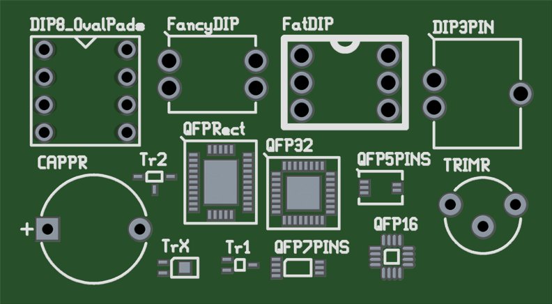
But sometimes one is missing, or you need a special kind of it. So you have to make your own. For PCB this is not too difficult -- the footprints are defined in textual form, which can easily be modified with a text editor. For creation of new footprints different tools exist, some which are command line driven, some with a graphical or web based interface. On this page yet another one is available -- command line based and written in Ruby. Here are a few arbitrary footprints which are built for some testing of this generator:
You may use these links to get the program (version 0.13) and testdata:
The generator script is called from the command line and needs an installed Ruby interpreter to do its work. Execute it by simple typing in its name in a (Linux/Unix) shell like "./sfg.rb" or by invoking the Ruby interpreter with this script by "ruby sfg.rb". If you call it without or with arguments "-h" or "--help" you get this help text:
stefan@AMD64-X2 ~/foo $ ./sfg.rb --help
sfg.rb -- yet another footprint generator for gEDA/PCB
Version: 0.12 (08-JUN-2009)
Author: S. Salewski
License: GPL

This is a plain footprint (land pattern) generator for gEDA/PCB
written in Ruby. The intention was to make its use simple, safe
and intuitive. Extension for new types of footprints is easy.

The program processes a textual input file, which contains the
parameters needed for generation of footprints. Each line of this
input file defines a single parameter, i.e. "pindiameter = 0.8 mm".

The input file is divided in sections by "Device = " statements.
You can define global parameters, if you prepend the parameters
with the line "Device = Global". Parameters specific for a special
type of footprint are defined if you prepend the parameter
definition by a command like "Device = DIP". In this case all
following parameter definitions are local. You may redefine global
parameters here, but after next "Device = " command all global
parameters have again their previous state (and no local parameters
exist). This behaviour ensures that insertion of a new section can
never influence existing sections. You can define a default unit,
so mm or mil for dimensions is optional. Equal sign for assignment
is optional too, or you may uses ":=". Numeric parameters can be
simple expressions like "2.1+0.8*2". If parameters are not numeric
and are not simple text strings, you should include it in quotation
marks. The command "Generate" followed by a filename will write the
footprint file to disk. This is a small piece of a configuration
file:

Device Global
  date "10-APR-2008"
  clearance 10 mil
  defaultunit mm

Device DIP
  defaultunit mil # locally overwrite a global parameter
  width = 300
  pins 8
  drilldiameter 0.8*1.1 mm # 10 % tolerance
  refdespos upperleft
  Generate "DIP8-300.fp" # this is a command, so do not use = sign.

If you execute this program with argument -h or --help then this
documentation is written to stdout. If you give a command line
parameter, this is considered as an input file and processing
starts. You can generate an empty input file (template) if you
give "PrintAll" as command line argument, or you may generate an
input template for a specific device by using that name, i.e.
"DIP" as argument. Redirect the output to a file and fill in the
missing information. (If you don't need the comments, then use
sed to filter the output, like "./sfg.rb List | sed s'\ #.*\\'".)

Supported device types:
-----------------------
DIP: http://en.wikipedia.org/wiki/Dual_in-line_package
SIP: Single In Line
QFP: http://en.wikipedia.org/wiki/QFP
CAPPR: Capacitor Polarized Round
TRIMR: Potentiometer or variable Capacitor, 3 pin through hole with Round outline
This should be enough information to use it. If you give the command line argument "List" you get something like this:
stefan@AMD64-X2 ~/foo $ ./sfg.rb List
Device = Global
  author = ""
  dist-license = GPL
  use-license = unlimited
  defaultunit = "" # mm or mil
  silkwidth = 10 mil # thickness of silk lines
  silkbox = "" # inner or outer for autosize, custom for explicit size, otherwise no box
  silkboxwidth = 0 mil # silkbox width, used if silkbox = custom, no box if value too small
  silkboxheight = 0 mil # silkbox height, used if silkbox = custom, no box if value too small
  silkoffset = 10 mil # distance between pads/pins and silk lines, ignored if silkbox = custom
  textpos = upperleft # position of reference designator, upperleft, few devices accept center
  textorientation = horizontal # horizontal, some devices may accept vertical
  refdessize = 100 # size of reference designator, default is 100 (integer)
  mask = 6 mil # distance between the copper of pads/pins and the mask
  clearance = 10 mil # distance between the copper of pads/pins and any polygon
  p1silkmark = "" # mark pin/pad 1 with silk: to get a mark use: mark, p1mark, yes, true, 1
  p1coppermark = "" # mark pin/pad 1 with copper: to get a mark use: coppermark, yes, true, 1
Device = DIP
  pins =  # total number of pins
  width =  # separation of the two columns of pins -- center to center
  pitch =  # distance between adjacent pins
  pad-dia =  # outer diameter of copper annulus
  drill-dia =  # diameter of the hole
  ovalpads = "" # to get ovals use: oval, ovalpads, yes, true, 1
  p1silkmark = "" # mark pin/pad 1: global, or specific shape: semicircle, notch, damage, slash
  p1coppermark = "" # mark pin/pad 1: global section, or for specific shape: square, octagon
  # Generate ?.fp
Device = QFP
  pins =  # total number of pins
  rows = 0 # number of pins at side of pin one -- 0 is identical to pins/4
  width =  # separation of the two columns of pads -- center to center. If 0 height is used.
  height =  # separation of the two rows of pads -- center to center. If 0 width is used.
  pitch =  # distance between adjacent pads -- center to center
  padthickness =  # should be smaller than pitch
  padlength =
  ovalpads = "" # to get ovals use: oval, ovalpads, yes, true, 1
  p1silkmark = "" # mark pin/pad 1: global section, for specific shape: circle, damage, slash
  # Generate ?.fp
Redirect this output to a file, fill in the missing data, and use it as the input file for the generator. If all goes well this should result in fine footprint files similar to this one:
Element["" "" "DIP8_OvalPads" "" 0 0 -19650 -27150 0 100 ""]
(
  Pin[-15000 -15000 6299 2000 7499 3937 "1" "1" ""]
  Pad[-16575 -15000 -13425 -15000 6299 2000 7499 "1" "1" "onsolder"]
  Pin[-15000 -5000 6299 2000 7499 3937 "2" "2" ""]
  Pad[-16575 -5000 -13425 -5000 6299 2000 7499 "2" "2" "onsolder"]
  Pin[-15000 5000 6299 2000 7499 3937 "3" "3" ""]
  Pad[-16575 5000 -13425 5000 6299 2000 7499 "3" "3" "onsolder"]
  Pin[-15000 15000 6299 2000 7499 3937 "4" "4" ""]
  Pad[-16575 15000 -13425 15000 6299 2000 7499 "4" "4" "onsolder"]
  Pin[15000 15000 6299 2000 7499 3937 "5" "5" ""]
  Pad[13425 15000 16575 15000 6299 2000 7499 "5" "5" "onsolder"]
  Pin[15000 5000 6299 2000 7499 3937 "6" "6" ""]
  Pad[13425 5000 16575 5000 6299 2000 7499 "6" "6" "onsolder"]
  Pin[15000 -5000 6299 2000 7499 3937 "7" "7" ""]
  Pad[13425 -5000 16575 -5000 6299 2000 7499 "7" "7" "onsolder"]
  Pin[15000 -15000 6299 2000 7499 3937 "8" "8" ""]
  Pad[13425 -15000 16575 -15000 6299 2000 7499 "8" "8" "onsolder"]
  ElementLine[-19650 -19650 -19650 19650 1000]
  ElementLine[-19650 -19650 19650 -19650 1000]
  ElementLine[19650 19650 19650 -19650 1000]
  ElementLine[19650 19650 -19650 19650 1000]
  ElementArc[0 -19650 3930 3930 0 180 1000]
  Attribute("name" "DIP8_OvalPads")
  Attribute("author" "Stefan Salewski")
  Attribute("dist-license" "GPL")
  Attribute("use-license" "unlimited")
  Attribute("date" "08-FEB-2009")
  Attribute("documentation" "www...")
)
One important note: The generator program is not much tested now. If you use it, carefully investigate the results, i.e. load the generated footprints into PCB program and make a printout. Arrange the electronic devices over the corresponding footprints to verify that they fit well. And verify the pin numbers inside of the PCB program. Please let me know if there are any problems.
Currently the program supports the basic types "DIP", "SIP" and "QFP". Expanding it to new types is not difficult: Expand the "datas" array which holds information for all devices, make a copy i.e. of the "GenDIP()" generator function, modify and rename it. And expand the function "Generate()" to call this new function. Some basic knowledge of the Ruby programming language and of the structure of PCB footprint files is sufficient to do this.
If you want to get some feeling of Ruby I recommend this fine tutorial:
If you want to learn the format of PCB footprint files, you may consult the really verbose description of Stuart Brorson:
Or you may read my short summary: